
Membranes move with Moore’s Law for semiconductors
Canatu, the manufacturer of advanced carbon nanotubes (CNTs) based in Vantaa, Finland, achieved an increase in sales of over 260% year-on-year in 2021, driven by its fast-rising semi-conductor business which accounted for 58% of total sales.
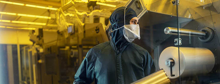
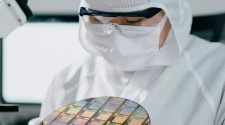
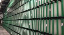
The company’s ultra-thin EUV (extreme ultraviolet lithography) membranes – only introduced in 2021 – are capable of filtering particles down to the nano scale and are now enabling a significant step forward in semiconductor manufacturing and efficiency.
CNTs
CNTs are one-atom-thick carbon sheets rolled into tubes. They can be single, double or multi-walled, vary in diameter and in length and be arranged in different configurations to form membranes of
different densities.
The learning curve with carbon nanotubes has recently been rapid, Canatu reports, and development has been supported by parallel progress in nanotechnology and other technological advances.
Canatu has now perfected a special floating catalyst chemical vapor deposition (FC-CVD) process for carbon nanotube manufacturing. Controlling the CNT growth during FC-CVD in mass production is challenging and for some years delayed the widespread use of CNTs, despite their remarkable properties. It is also the reason why CNTs from a vendor can vary largely from batch to batch – a barrier Canatu says it has now successfully overcome. The dry deposition process results in cleaner, longer and practically defect-free carbon nanotubes compared to liquid dispersion methods.
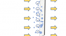
During Canatu’s FC-CVD process, catalyst particles are created at the top of the reactor. These particles float downwards with a carrier gas towards a membrane filter. As the catalyst particles flow through the reactor, carbon nanotubes grow on the catalyst particles before landing directly on the filter, forming the CNT film. The benefits of this method include being low-cost, readily scalable and enabling enhanced control of CNT growth to ensure optimal film and membrane performance.
Since 2020 the semiconductor industry has been in crisis, with demand exceeding the supply and impacting at least 169 industries.
Films and membranes

For CNT films, the deposited carbon nanotubes are transferred from the collection filter to a plastic substrate film, before being chemically functionalized. Chemical functionalization serves to improve the conductivity and stability in the films, whilst improving sensitivity and selectivity in electrochemical sensors.
For free-standing CNT membranes, the deposited carbon nanotubes are transferred to a frame before going through post-treatments which serve to modify or enhance properties. Densification can be carried out for EUV pellicles, for example, to ensure better adhesion of the carbon nanotubes to the frame material. The final step of the manufacturing process for both CNT films and free-standing CNT membranes involves inspecting and testing the final product before sending the approved pieces to be packaged.
Canatu now has 20 years of experience in carbon nanotube manufacturing with FC-CVD, and almost ten years of experience in mass-producing the high-quality carbon nanotubes for the most demanding applications.
Semiconductors
Semiconductors are to be found in every single electronic device on the market and since 2020 the industry has been in crisis, with demand exceeding the supply and impacting at least 169 industries. The crisis has led to major price increases, shortages queues and scalping among consumers for cars, graphics cards, video game consoles, computers and many other products.
The global semiconductor crisis is attributed to a combination of different events with the snowball effect of the COVID-19 pandemic being the primary reason for accelerating shortages.
Another contributing factor is that demand is so great that existing production capacity can’t keep up and other causes have been attributed to the China-United States trade war and the 2021 drought in Taiwan.
Nevertheless, progress in the industry continues to be driven by Moore’s Law which dictates that the transistor density on a wafer must double every two years. Higher transistor density leads to more efficient processors and memory chips for the benefit of everyone using electronic devices. Gordon Moore’s observation-turned-law has been used in the semiconductor industry to guide long-term planning and to set targets for research and development since 1975.
EUV
To keep up with the pace of development, the industry has developed extreme ultraviolet lithography (EUV) technology. Using extreme ultraviolet wavelengths, this wafer exposure technology improves resolution and allows wafers to be produced with transistor node sizes of 7nm or less. EUV lithography technology provides an optimal choice for next generation applications such as 5G, AI and the automotive industry.
As volumes rise in semiconductor manufacturing and ever-smaller features are printed on them, there is a greater pressure to avoid defects – tiny defects lead to errors on the wafer, causing costly yield losses.
Canatu has developed a unique solution based on free-standing CNT membranes to enable nanoscale debris filtering in a demanding environment – with high EUV transmittance, low reflection and flare, high
heat resistance and mechanical strength.
EUV pellicles are membranes that protect the photomask from particle contamination while permitting EUV transmission. The free-standing CNT membrane must be thin enough to limit the imaging impact
while robust enough to survive handling.
In addition to protecting the photomask from defects, the EUV pellicles enhance precision, shorten processing and increase production efficiency on the wafer by around 25%
Defects in printing remain a key constraint to EUV lithography uptake and the build-up of tiny dust particles on a photomask (reticle) can lead to printing errors, making a sophisticated particle filter essential.
The key properties of Canatu’s EUV pellicles a 97% transparency at EUV, high heat stability, robustness to pressure differentials, nanoscale filtering capabilities and high uniformity.
Development
It was only in October 2020 that Imec, a leading research and innovation hub for nanoelectronics and digital technologies based in Leuven, Belgium, announced its promising new results in EUV reticle protection.
Multiple CNT-based pellicles were mounted on reticles and exposed in an NXE:3300 EUV scanner at imec, demonstrating the successful fabrication and scanner handling of full-field CNT-based pellicles. The tested pellicles had a single-pass EUV transmission up to 97%. The impact on imaging was found to be low and correctable based on critical dimension (CD), dose, and transmission measurements.
During high-volume semiconductor manufacturing, the pellicle is mounted a few millimeters above the surface of the photomask so that if particles land on the pellicle, they will be too far out of focus to print. Developing such an EUV pellicle was very challenging, since 13.5nm light is absorbed by most materials. In addition, stringent thermal, chemical, and mechanical requirements had to be achieved. Such highly transparent pellicle is critical to enable high yield and throughput in advanced semiconductor manufacturing.
Since 2015, imec had worked with selected CNT suppliers including Canatu, to develop membranes meeting EUV pellicle targets for properties like transmittance, thermal durability, permeability, and strength and to enable the imaging results.
Expansion
This success is reflected in Canatu’s 2021 results, and the company is anticipating a further growth of over 70% in the first half of 2022, as the take-up for advanced EUV membranes in the semiconductor industry continues to escalate.
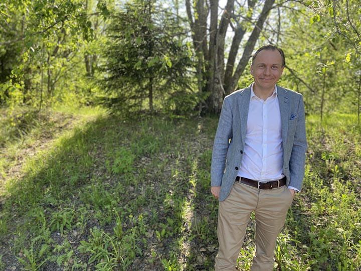
“The demand for EUV membranes is being spurred by the trend towards smaller node sizes and a greater pressure to avoid defects,” says Samuli Kohonen, vice president of sales at Canatu. “Tiny defects lead to errors on the wafer causing costly yield losses. If we are to keep up with Moore’s Law, the throughput of EUV machinery now needs to move even closer to high-volume manufacturing.”


