
Water, so critical to life, has been present in roughly the same quantity on this planet for millions of years. We are neither gaining nor losing water. Unfortunately, humankind is doing a great job of contaminating this fixed quantity of water.
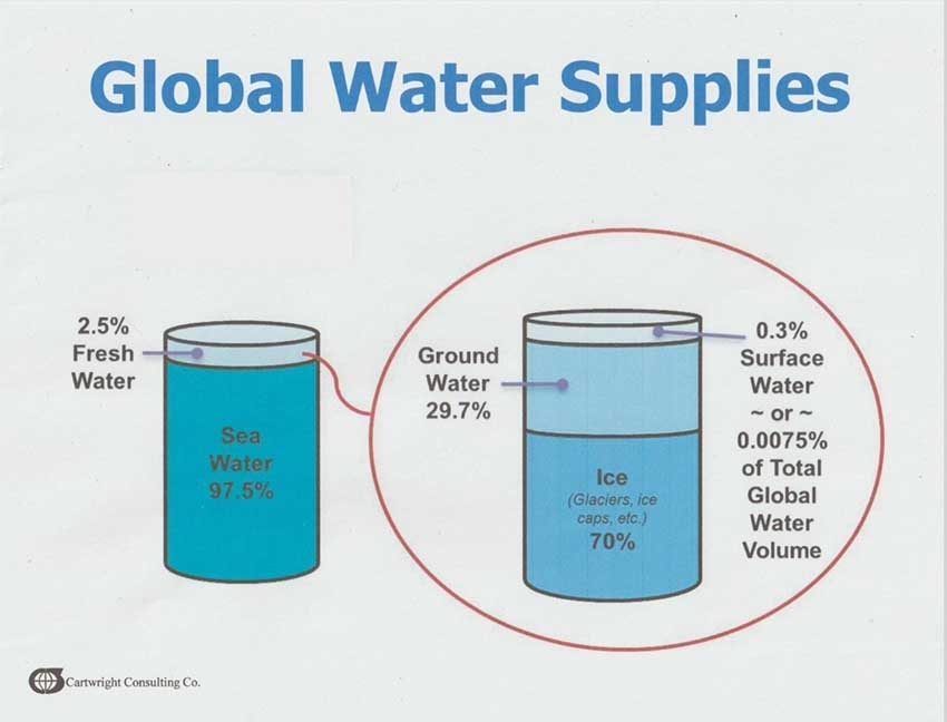
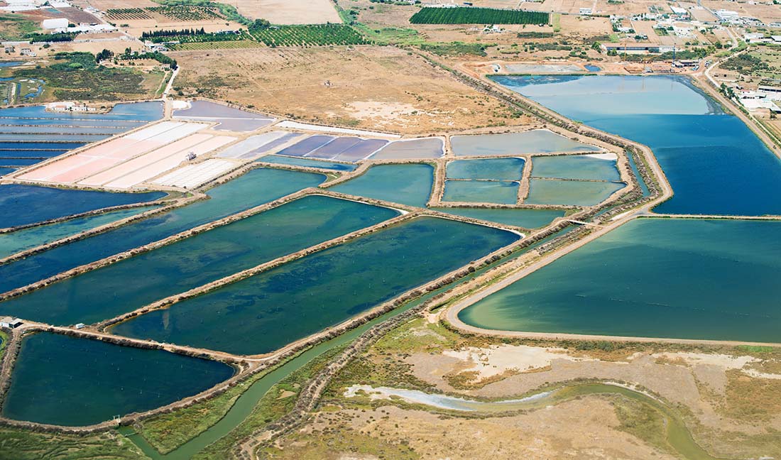
Figure 1 indicates the availability of global water accessible for human activities.
Note that only about 30% of the fresh water is available (not frozen), and most of that is in aquifers, some of which are difficult to access.
No two sources of water have identical contaminant types or concentrations, and as population growth increases, our existing water supplies are becoming more polluted.
Global warming is affecting precipitation frequency, intensity, and location, thereby disrupting the availability of water, regardless of quality.
Continuing improvement of chemical analyses have enabled scientists to identify a growing list of emerging contaminants, revealing that water supplies are much more contaminated than previously thought, albeit with tiny amounts of heretofore unidentified contaminants. The smaller the concentration we can measure, the more we find.
Although the chemistry of water contaminants is very diverse, they can be categorized into the following groups:
- Suspended solids
- Dissolved ionic salts
- Dissolved organic compounds
- Dissolved gases
- Microorganisms
As each of these groups may require a different suite of treatment technologies for optimum removal, the total water treatment system requires a relatively complex design. The specific contaminants (and their concentrations) in a given water supply can also complicate the system design.
Fortunately, the water treatment industry is constantly developing new technologies and today, there is virtually no contaminated water or wastewater supply that cannot be treated to meet virtually any quality requirement.
Water Quality
According to a report from Precedence Research, the global semiconductor market size was estimated at $628 billion in 2025 and is expected to reach $1207 billion by 2034, with a CAGR of 7.54%.
By one estimate, this industry uses 12 gallons of ultrapure water to rinse one square inch of wafer, and given that this application demands the highest-quality water possible, an even greater understanding of water treatment processes is required.
As stated, the water used in semiconductor manufacturing must be of the highest quality; in reality, it cannot be pure enough. Quality requirements are pushing the envelope of innovative water treatment technologies, and the plethora of contaminants and their concentrations present a significant challenge to the system designer.
The industry has developed a standard, ASTM D127-13, “Standard Guide for Ultra-Pure Water Used in the Electronics and Semiconductor Industries.” It lists recommended quality requirements based on device line width: the smaller the line width, the higher the quality of water required. All of the above contaminant groups are addressed, and the contaminant values are generally limited by the accuracy of analytical measurements.
This standard is not mandatory, but offers suggested guidelines. Many manufacturers have developed their own quality standards.
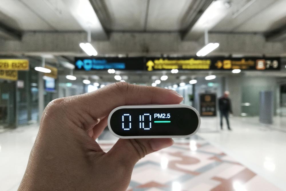
Given that analytical chemists are now measuring contaminant concentrations in the nanogram/liter (ppt) range, it is reasonable to expect this standard to be revised to include even more stringent requirements. To put it into context, one ppt is equivalent to one second in 32,000 years.
Herein, the focus is on the technologies for Type E-1.3 water used in the production of devices with line widths ranging from 0.032 to 0.065 µm.
Treatment System Design

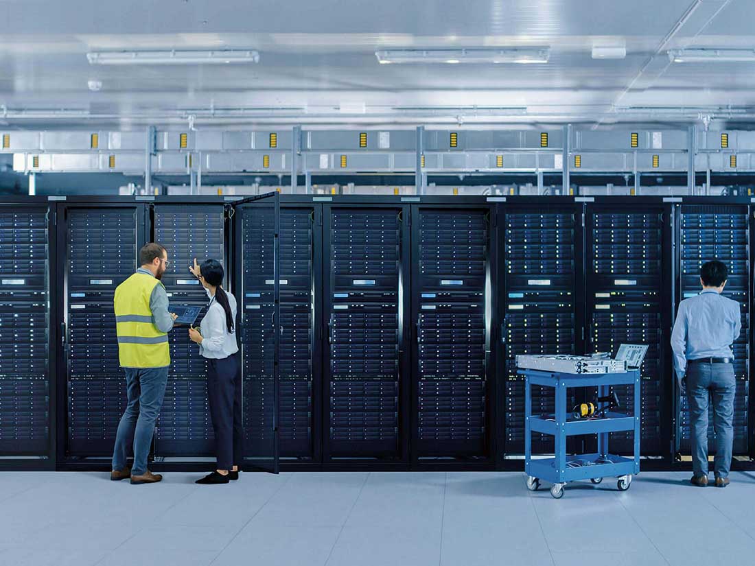
Figure 2 is an illustration of a water treatment system for producing semiconductor rinse water. It is separated into three units: Pretreatment, Primary Treatment, and Polishing. The Raw Water source is assumed to be municipal or a dedicated well. Treated wastewater is included in the influent to the treatment system.
In many cases, there are several technology choices for these components; however, the ones described are based on this writer’s years of experience.
Pretreatment
MEDIA FILTRATION
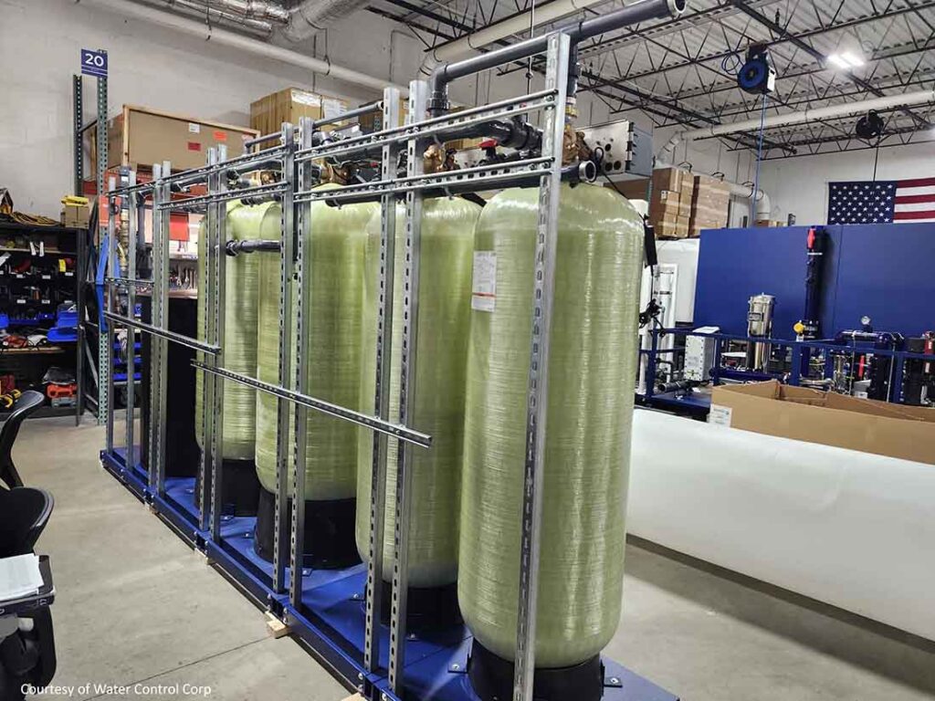
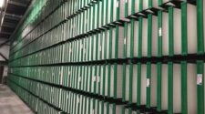
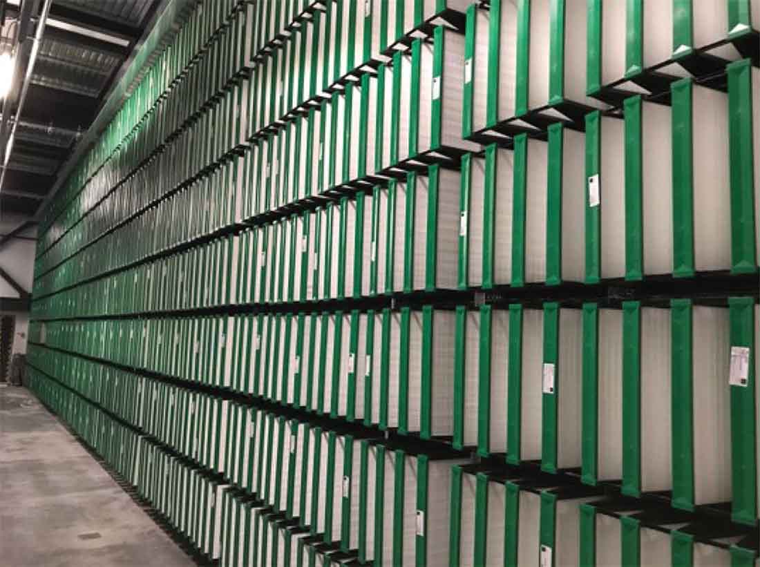
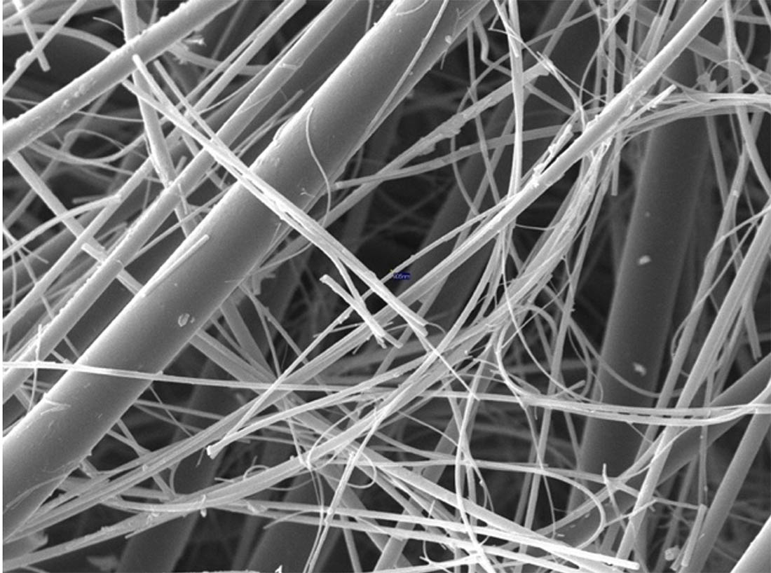
The level and size of suspended solids in the raw water will dictate the type and micron rating of the prefilters (Figure 3). Generally, surface water sources contain higher concentrations of suspended solids than groundwater, and for large volumes of water, bed filters containing media such as sand, anthracite, and/or other filter media are effectively utilized. The purpose of this treatment is to minimize the fouling or plugging of downstream technologies by suspended solids.
ACTIVATED CARBON FILTRATION (GAC)

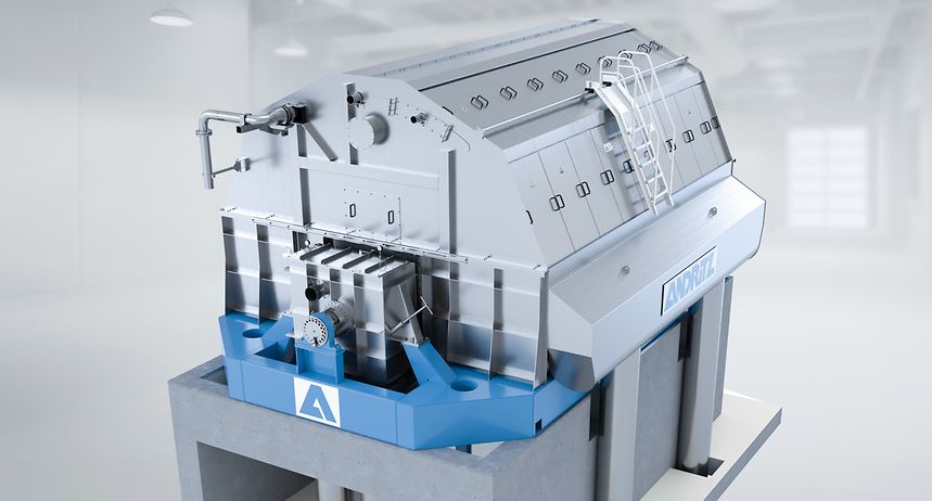
If the incoming water is from a municipal water treatment facility, it will contain a disinfectant (usually chlorine or chloramines) that must be removed prior to the reverse osmosis membranes (Figure 4). Granular activated carbon (GAC) filtration will also reduce some organic contaminants, which could foul the reverse osmosis membranes.
Primary Treatment
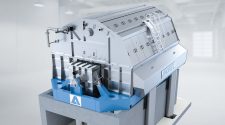
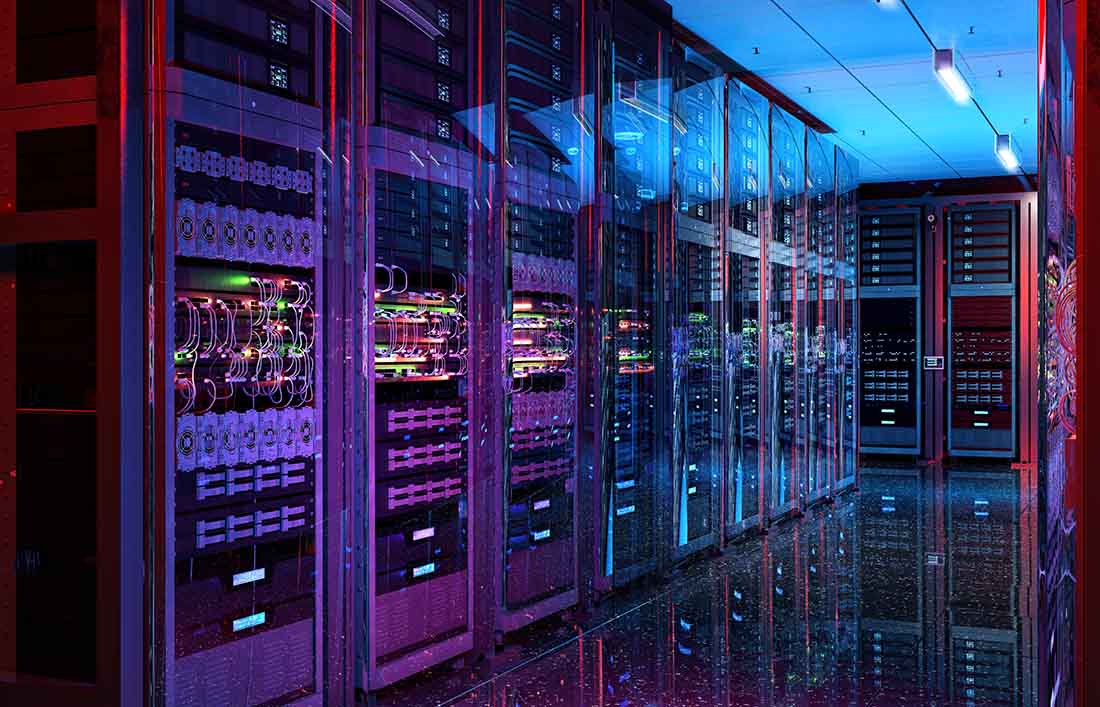
REVERSE OSMOSIS TECHNOLOGY (RO)
RO technology removes dissolved salts, dissolved organics (above 150 molecular weight) microorganisms, and virtually all traces of suspended solids. It is essentially atomic filtration, and in semiconductor applications, RO removes the bulk of contaminants but requires polishing technologies to achieve ultimate water quality (Figure 5).

ULTRAVIOLET IRRADIATION (UV)
UV is a viable technology for inactivating (destroying) microorganisms. 185 nm wavelength UV is used for both microorganism destruction and for breaking some chemical bonds of low-molecular-weight organics not removed by RO. 254 nm wavelength UV is primarily for microorganism destruction (Figure 6).

STORAGE TANK
The treated water is somewhat aggressive (corrosive) so it should be contained in an inert plastic (such as PVDF) or stainless steel (316L) tank. A nitrogen blanket within the tank usually replaces the air to keep oxygen out of the tank. It is recommended that a low concentration of ozone (~0.5 mg/L) be maintained in the tank to minimize microbial growth.
Polish
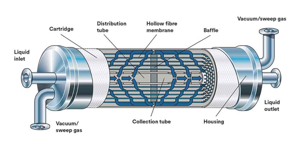
DEGASIFICATION
This component removes dissolved oxygen and carbon dioxide from the treated water. The latest technology is a membrane process that uses hollow-fiber membranes to absorb and remove the gases. This technology improves on traditional vacuum degasification (Figure 7 and 8).

ELECTRODEIONIZATION (EDI)
EDI offers significant advantages over the mixed-bed DI technologies formerly used to produce 18.2 megohm-cm resistivity (ionic quality) of Type E-1.3 water (Figure 9). Utilizing electricity as the energy source it requires no regeneration and produces a small wastewater stream while removing ionic contaminants and some TOC (total organic carbon).

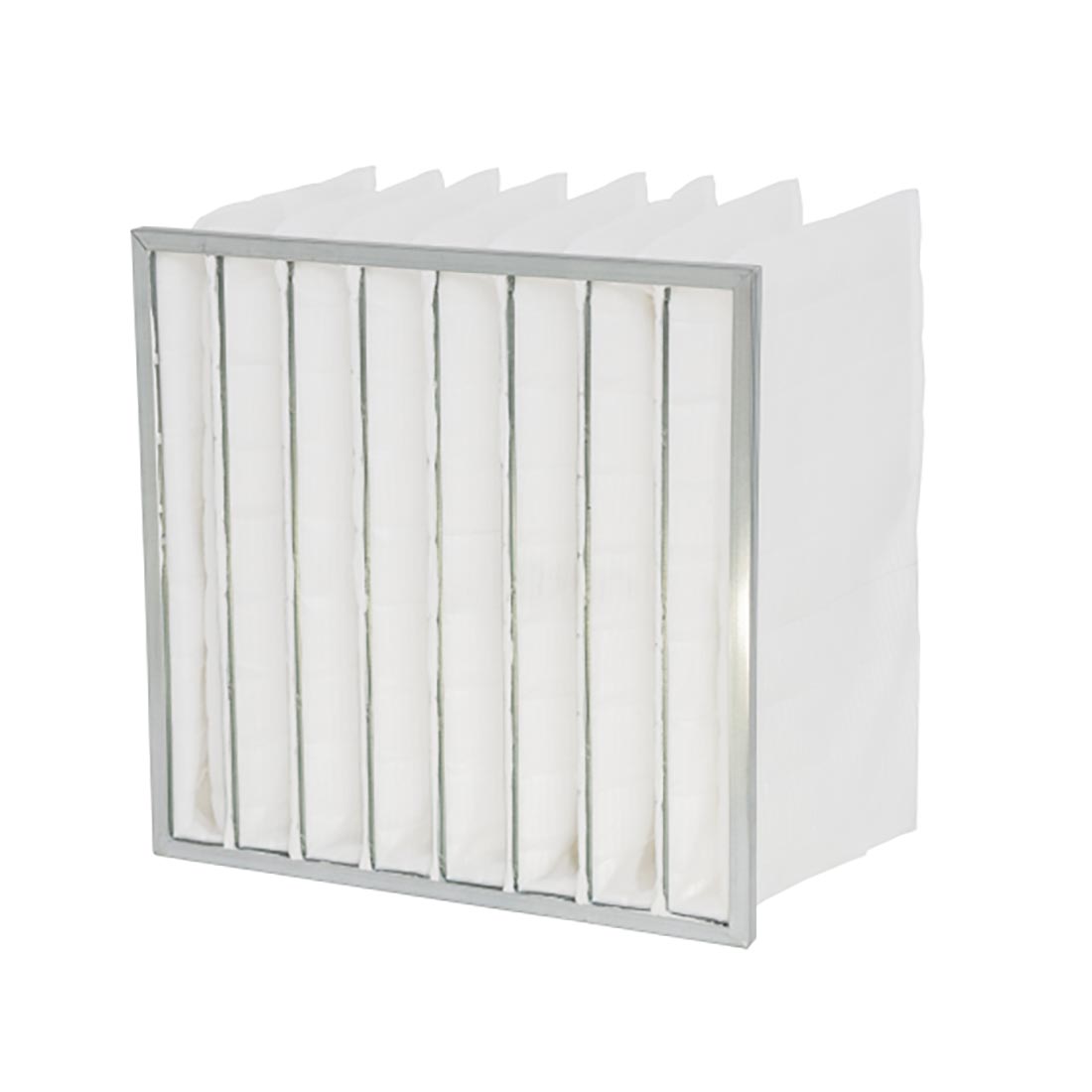
FINAL FILTRATION
Ultrapure water is highly aggressive and wants to dissolve everything in sight. Although the treatment technologies and storage and distribution components are made from inert construction materials, some contamination is always released from them. Additionally, microorganisms, particularly bacteria, are a major source of trace contamination. They contribute to TOC, ionic, and suspended solids contamination. There is more on these issues further in the article.
Ultrafiltration (UF) is a membrane technology designed to remove dissolved organics and very small suspended solids (<0.10 µ). Like RO, it uses a membrane to remove both on a continuous basis. UF generates a small waste stream containing these rejected contaminants. The pore sizes are listed as MWCO (molecular weight cutoff, the smallest molecular weight of an organic compound removed). Many different device configurations and polymers are available.
Most UF configurations allow for backwashing to remove accumulated fouling material.
Figure 10 illustrates a small skid-mounted complete treatment system.

Microorganism Issues
This group of contaminants commands special attention.
The normal water-borne microorganisms are protozoa, bacteria, viruses, algae, and fungi. They are all viable—self-propagating, but the most troublesome are bacteria. There are estimated to be 5×1030 bacteria on this planet.
About 98% of water-borne bacteria form biofilms, organic, lipopolysaccharide polymers that enclose and protect the bacteria from attack by disinfectants and cleaning chemicals. Bacteria want to attach to virtually all surfaces, including filtration media, membranes, and the inside walls of piping and tankage. This is the “scum” that forms on the sides of a container holding water for any length of time (think of the water dish for your dog or cat).
Not only do biofilm cover and protect the bacteria, but some sloughs off and contributes to TOC (total organic carbon). Dead bacteria (endotoxin) contribute suspended solids, TOC, and some ionic contamination to the water supply. Membranes (RO and UF), UV, ozone and EDI can all be utilized to minimize microorganism contamination.
It is virtually impossible to prevent microorganism (mainly bacteria growth; the realistic goal is to keep these concentrations low enough to meet the water quality requirements.
Wastewater Recovery and Reuse
As stated prior, with today’s water treatment technology and engineering expertise, there is no contaminated water supply that cannot be treated to meet any water quality standard, so let’s take a look at the wastewater leaving semiconductor manufacturing processes.
According to the reference: “Semiconductor manufacturing wastewater challenges and the potential solutions via printed electronics.1 The manufacturing of semiconductors involves more than 400 chemical products, and the IC fabrication process as a whole generates substantial volumes of wastewater containing a wide array of hazardous chemical pollutants including heavy metals, acids, alkalis, solvents, and other toxic substances.” This reference includes the statement that “…nearly all products (about 98%) contained trade secret ingredients…” The good news is that although the “ingredients” may be secret, they are certainly included in the contaminant groups listed above and can be removed from the wastewater with the same technologies.
The challenge is not the ability to remove these wastewater contaminants to meet ultrapure water quality standards; it’s a matter of economics.
By one estimate, grinding and cutting, Chemical-Mechanical Planarization, and hydrofluoric acid dis-
charge account for more than 50% of the wastewater volume. The wastewater treatment industry is well-positioned to effectively remove these and prepare them for safe disposal. Some chemicals, such as silica, volatile solvents, and certain recalcitrant compounds, are difficult to remove, but technologies exist to remove them.
It is possible to further treat the concentrated waste material and even produce “dry” solids; however, energy-intensive technologies such as crystallization and evaporation will likely be required.
Of course, landfilling is also a possibility, but some waste may require hazardous materials treatment, usually based on local regulations.
It is important to note that recovering and reusing wastewater from semiconductor manufacturing is not a “piece of cake” and will likely involve thorough testing and/or piloting, but it should not be held up as an impossible task requiring undeveloped technologies.
PFAS (per- and polyfluoroalkyl substances) have gained notoriety in recent years because they are ubiquitous in the environment, and two (of more than 16,000 PFAS compounds) have been listed on the EPA Primary Standards list for drinking water. Everybody has heard of these “forever chemicals,” which supposedly cannot be broken down, and the semiconductor industry has adopted the position that the PFAS they use cannot be replaced. In reality, technologies have been developed to break PFAS down into their basic chemicals (water, carbon dioxide, fluoride), and they will certainly be employed at municipal drinking water plants when the law goes into effect in 2031. Humans are very innovative, particularly when money can be made.
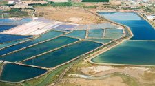
As an example of this innovation, the “poster child” for wastewater recovery and reuse in the U.S. is the Orange County Groundwater Replenishment System located in Fountain Valley, CA, touted to be the world’s largest water purification system for indirect potable reuse. Since 2008, it has processed secondary treated municipal sewage into 130 million gallons per day supplying drinking water to over one million people. Motivated by the chronic water shortages in the Western U.S., coupled with sea water intrusion contaminating the drinking water aquifers, the success of turning sewage into drinking water is a testament to an outstanding public relations initiative that overcame the “toilet to tap” mindset of their customers.
Concomitant with that is the recent revelation that Samsung Semiconductor has announced plans to use sewage to help supply its demand for almost one billion gallons per day of ultrapure water.
Conclusion
According to the SIA (Semiconductor Industry Association), “Semiconductors are a marvel of modern technology and the foundation of our digital world.” Such developments as chiplets, advanced packaging, backside power delivery, and numerous new materials, combined with quantum computing and AI, and buoyed by the Chips Act investment, give a strong indication that this industry is on the verge of explosive growth.
Water, with its fixed volume and increasing contamination threat, represents a potential limitation working against this growth. We must be able to access all water sources and economically treat them to meet the quality standards for both today’s products and those of the future. The rapid deployment of data centers, with their significant cooling water requirements, will underscore the value of recovered water and spur innovation.
Hopefully, this article provides guidance and direction to assist those challenged by addressing the water quality and quantity needs of the Semiconductor Industry today and into the future.
1 https://doi.org/10.1016/j.isci.2025.113576, October 17, 2025.


